
Y . -F. Wu1, D. Kebort1, J. Guerrero1, S. Yea1, J. Honea1, K. Shirabe2 and J. Kang2
Abstract
We present the first kW-class 3-phase GaN-based inverter hard-switched at 100-kHz PWM. The heart of the inverter is a 6-in-1 power module built with 600-V GaN power HEMTs. Each GaN transistor operates in three states including forward blocking, forward conducting and reverse conducting, eliminating the need for free-wheeling diodes. The high PWM fre- quency enables on-board compact filters, resulting in high-quality pure sine-wave motor- drive power. A high inverter efficiency of 98.5% was achieved and motor electro-mechanical efficiency improvement by >2% was also observed.中国电力电子产业网
1. Introduction
In the last decades Si-based power switching devices have been improved to a highly ma- tured stage. As an impressive example, Si super-junction MOSFETs such as CoolMOS FETs broke the theoretical Si limit in the tradeoff between blocking voltage and on re- sistance [1]. However, the large amount of minority charge in the body diode results in large reverse recovery losses in hard-switched bridge circuits typical for motor-drive inverters. As a result, insulated-gate-bipolar-transistors (IGBTs) are preferred in such applications which also require additional reverse connected diodes for free-wheeling current. With the rela- tively-low frequency bandwidth, IGBT-based inverters typically operate at 4-20 kHz and di- rectly apply Pulse-Width-Modulation (PWM) power to the motor with the intention to utilize the motor windings as energy storage inductances. The resultant voltage transients induce high stresses between motor windings and cause current spikes through motor bearings, leading to issues of insulation breakdown and excessive bearing wear [2][3]. In this paper, we demonstrate the use of wide-band-gap semiconductor GaN for hard-switched motor- drive applications. The functionalities and frequency capabilities of the GaN High Electron Mobility Transistor (HEMT) eliminate the need for free-wheeling diodes and allow a much higher PWM frequency which enables compact filters and resultant spike-free pure-sine- wave power output.中国电力电子产业网
2. Devices & Module
The unit cell device used in this study is a GaN hybrid HEMT produced by Transphorm Inc. It incorporates a normally-off low-voltage Si device at the input and a normally-on high- voltage GaN HEMT at the output in a cascode form as seen in Fig. 1. The combined device is normally-off having a gate threshold of +2.1V typical at 1mA drain current and a drain leakage of 10A typical at Vgs=0V & Vd=600V. The on-resistance is 0.15 typical and pulsed drain current is 70A. This 1st generation GaN device not only exceeds the pe rfor- mance of the best competing Si MOSFETs in terms of on-resistance, switching speed and parasitic capacitances, but also is capable of operating in reverse conduction mode with lit- tle reverse recovery charge (Qrr). As seen in Fig. 2, with gate-source shorted, reverse re- covery charge of a fast-recovery CoolMOS FET and a GaN hybrid HEMT with similar on- resistances and current ratings were tested from a reverse conduction of 9A current to fo r- ward blocking of 400V. It is clear that the GaN device cuts the Qrr by 25 times. Because of these properties, the GaN FET is a strong candidate for high-frequency hard-switched bridge topologies and can achieve the function without a free-wheeling diode. Fig. 3 com- pares two 3-phase bridge circuits using Si IGBTs and GaN HEMTs. In addition to expected efficiency and frequency benefits, the GaN implementation slashes the high-voltage device count by half, significantly simplifying the inverter circuit.中国电力电子产业网
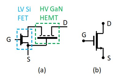
Fig. 1. Hybrid HEMT incorporates a low-voltage normally-off Si FET and a high-voltage normally-on GaN HEMT (a) to achieve a combined, normally-off device (b).
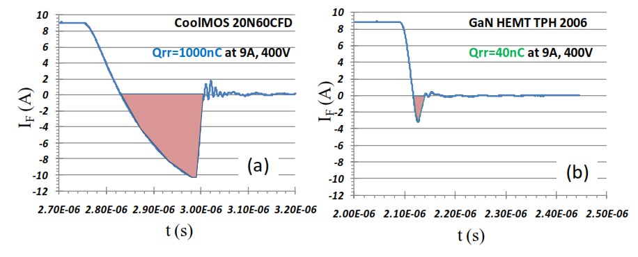
Fig. 2. Reverse recovery charge test result for (a) a fast-recovery CoolMOS and a Transphorm GaN HEMT, showing a reduction of Qrr by 25 times by GaN. Note that the current transient is 450A/s for the GaN HEMT and only 100A/s for the CoolMOS due to the excessive ringing at higher dt/dt values.中国电力电子产业网
A 6-in-1 module was engineered using these GaN device cells with the schematics and package photo shown in Fig. 4. The module design follows high-frequency circuit principles and features Kelvin source leads for stable gate drives to ensure misfire-free high dV/dt op- eration. Based on device specifications, the module is capable of 600 V blocking voltage and 14 A of continuous operation current for each switch at a case temperature of 100 oC. Each half bridge was inductively switched to confirm a current handling capability greater than 18 A at a rail voltage >400 V.
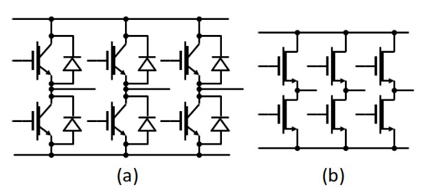
Fig. 3. Schematics of 3-phase bridge circuits using (a) IGBTs & fre-wheeling diodes, and (b) GaN HEMTs without diodes中国电力电子产业网
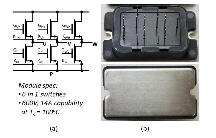
Fig. 4. (a) GaN module schematics and (b) packaged module.
3. Inverter & Performance中国电力电子产业网
A 3-phase inverter was constructed using the GaN power module based on the schematics shown in Fig. 5. Texas Instruments’ TMS320F28069 DSP was chosen to generate high- resolution PWM signals at 100 kHz. Three complementary PWM peripherals were config- ured to generate the non-overlapping pulses to each of the three transistor pairs forming the bridge. A dead-time of 62.5 ns was directly inserted by the PWM peripheral. Space vector modulation was used to intentionally introduce odd harmonics instead of pure sinus- oidal envelops to maximize usage of the DC rail voltage. A start up sequence with constant V/Hz was incorporated for driving induction motors from zero to rated rotation speed. Low- cost sand-dust power core inductors and SMD ceramic capacitors were used for the com- pact L-C filters (Lu/Cu, Lv/Cv & Lw/Cw). A photo of the finished inverter is shown in Fig. 6. The outer dimensions are about 4” x 4.5” x 1.6” without a heat sink. With some optimization, a heat sink can be fitted to the same volume.中国电力电子产业网
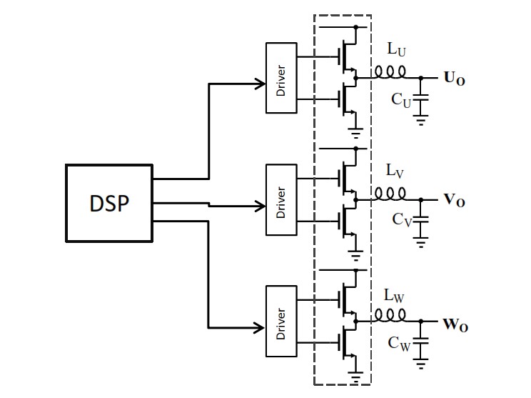
Fig. 5. Simplified schematics of the 3-phase high-frequency GaN inverter. The module is indicated with the dotted box. Lu &Cu (200uH & 0.3uF) form a compact filter. UO, VO & WO are the three output terminals.中国电力电子产业网
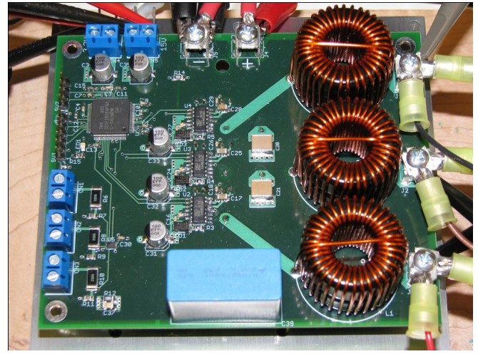
Fig. 6. Photo of the 2-kW, 3-phase GaN inverter operating at 100-kHz PWM with on-board compact filters for pure-sine-wave output.
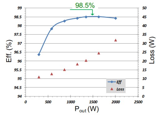
The inverter was tested at a dc rail of 350 V and a PWM frequency of 100 kHz. Fig. 7 (a) shows voltage output waveforms of all three phases after the L-C filters as referred to the negative rail. The odd harmonics are apparent as mentioned before, which were inte ntional- ly introduced to fully utilize the dc potential. The line-to-line voltages fed to the delta-connected loads are sinusoidal as seen in Fig. 7 (b). In contrast to conventional motor drive outputting high-voltage PWM power, the GaN inverter generates pure sine-wave power without a bulky filter. This allows motors to be operated with ideal excitations hence an im- proved electro-mechanical efficiency and reduced bearing wear. The inverter performance was tested with resistive loads as seen in Fig. 8. Even hard-switched at a high PWM fre- quency of 100 kHz and with low-cost sand-dust inductors, the GaN inverter is capable of high efficiencies up to 98.5%. This performance obtained at such a high switching frequen- cy for a true dc-to-sine-wave inverter cannot be achieved with traditional semiconductors.中国电力电子产业网
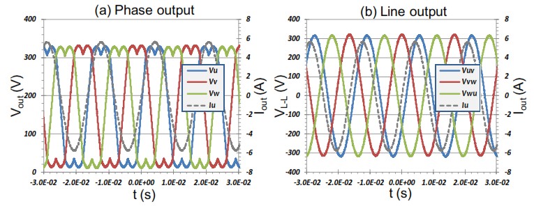
Fig. 7. Output voltage waveforms of: (a) each phase referred to the negative rail; (b) line-to-line.
4. Electro-mechanical Test
The GaN inverter was then evaluated in a motor drive test lab at Yaskawa America, Inc. The test motor was model MTRY541 by Marathon Electric, rated at 2.2kW. A 2.2-kW Si- based motor-drive inverter (A1000 series, model CIMR-AU2A0012FA) operating at 15-kHz PWM frequency without an output filter (reactor) was used for a direct comparison to the GaN inverter. It employed an IGBT power module CP30TD-12A rated at 600V 30A. Both in- verters were configured to be fed with 320 Vdc and produced 225 Vrms 3-phase ac output at 60Hz. Electrical power was measured by a WT1800 Yokogawa power analyzer and the mechanical power by a torque transducer power meter. The system was loaded in steps of 0.2kW up to the rated power. Fig. 9 shows the electrical performance as a function of load. Although operating at 7x high PWM frequency and including output filter losses, the GaN inverter was able to match the IGBT inverter efficiency at 2kW and outperformed it at lower load. The reduced overall efficiency compared to the case of resistive load (Fig. 8) is due to the non-ideal power factor of the motor.中国电力电子产业网
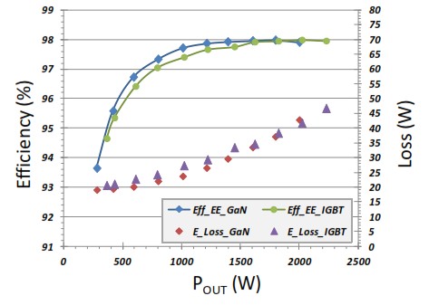
Fig. 9. Electrical efficiency as a function of output power for the GaN inverter at 100kH and the IGBT inverter at 15 kHz PWM. The efficiency for the GaN inverter includes output filter loss while the IGBT inverter has no output filter.
The main advantage of the GaN converter is its pure sine-wave output apparent in the mo- tor current waveform shown in Fig. 10. The direct PWM power from the IGBT inverter led to substantial high-frequency contents in motor current, causing higher dissipations in the mo- tor windings and iron cores. In contrast, the on-board compact filters (enabled by the high PWM frequency) in the GaN inverter resulted in smooth pure sine-wave drive current. Com- pelling benefit of this sine-wave output is revealed in the motor efficiency plots as a function of load for both IGBT and GaN inverters (Fig. 11a). The improvement in motor efficiency is 8% at low load, ~4% at mid load and >2% at full load. This directly translates to markedly improved system efficiencies (Fig. 11b) hence substantial energy savings. The high quality drive power will also prolong motor life as a result of less bearing wear from absence of cur- rent spikes and a cooler operation temperature from reduced self heating.中国电力电子产业网
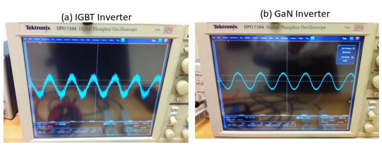
Fig. 10. The motor current waveform when driven with a (a) IGBT inverter and (b) with a GaN invert- er.
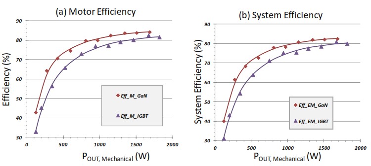
Fig. 11. Electro-mechanical performance using IGBT inverter and GaN inverters. (a) Motor efficiency vs. load and (b) System efficiency vs. load. The pure sine-wave output from the GaN inverter substantially improved motor efficiency.
5. Summary
A diode-free 6-in-1 GaN power module with 600-V rated voltage and 0.15- on resistance was developed. A 3-phase inverter was successfully built to operate up-to 2 kW at a PWM frequency of 100 kHz with high efficiency up to 98.5%. The high PWM frequency enabled compact on-board filters resulting in pure-sine wave output power. The spike-free output waveform substantially reduced motor losses, increasing system efficiency by 8% at low load and >2% at high load. This application example clearly demonstrates the promise of GaN power electronics in motor applications.中国电力电子产业网
6. Aknoledgement
This project was funded by ARPA-E and monitored Dr. Rajeev Ram and Dr. Pawel Gradzki.
7. Literature
[1] Deboy, G. et al. A New Generation of High Voltage MOSFETs Breaks the Limit Line of Silicon. Proc. IEDM. 1998, p.683-685. [2] Bearing currents in modern AC drive systems, ABB Technical Guide No. 5. http://www05.abb.com/global/scot/scot201.nsf/veritydisplay/8c253c2417ed0238c125788f003cca8e/$fil e/abb_technical_guide_no5_revc.pdf [3] Motor bearing current phenomenon, Yaskawa Application Note AN.AFD.17 http://www.yaskawa.com/site /dmdrive.nsf/(DocID)/NKOE-7HA2UX/$File/AN.AFD.17.pdf中国电力电子产业网
Fig. 8. Efficiency and loss as a function of output power to resistive loads (digital control & filter loss included).
热搜关键词:中国电力电子产业网 功率二极管 电力电子 IGBT