Reduction of Turn-off Loss in 600V-class Superjunction MOSFET by Surface Design
T. Tamura, M. Sawada, Y. Onishi, S. Watanabe, T. Shimatou, and T. Kobayashi
Fuji Electric Co., Ltd., 4-18-1, Tsukama, Matsumoto, 390-0821, Japan.
E-mail: tamura-takahiro@fujielectric.co.jp
Abstract
In purpose of making power MOSFETs more efficient in electric equipments, we have demonstrated 600V-class superjunction (SJ)-MOSFETs with excellent switching performance trade-off between turn-off loss (Eoff) and turn-off dV/dt. The fabricated SJ-MOSFET with the on-resistance of 0.10Ω at the breakdown voltage (BV) of 680V achieved the Eoff of 160uJ at the turn-off dV/dt of 10kV/us by optimizing a gate-todrain capacitance (Cgd) and a threshold voltage (Vth). This is about 40% lower turn-off loss than that of an unoptimized one. The power efficiency using the fabricated SJMOSFET reached over 94.0% in a 400W-class power supply.
1 Introduction
In recent years, with increasing concerns of environmental issues, electric equipments have been attracting attention as a way to achieve energy savings and resource conservation. In order to reduce the power loss of electric equipments, the power converters in electric equipments must be made more efficient. This leads to strong demand for power MOSFET with both low conduction loss and low switching loss. To address this requirement, SJ-MOSFET has been used in power converters because of their excellent trade-off characteristics between specific on-resistance (RonA) and BV, and their market has been rapidly expanding year by year. SJ-MOSFET is comprised of alternating n/p-pillars in drift region and can achieve low on resistance by increasing the drift region doping concentrations, narrowing the n/ppillar widths [1, 2]. Many researchers have improved RonA-BV trade-off relationships. RonA of SJ-MOSFETs by 1/3 to 1/5 compared to that of conventional MOSFETs have been realized [3, 4].
However, SJ-MOSFETs have an issue on the Eoff-turn-off dV/dt trade-off. This is due to the fact that SJ-MOSFET after the pinch-off in n/p-pillars has a small Cgd than that of a conventional MOSFET in case of the same on-resistance. Too small Cgd leads to high turn-off dV/dt and degrade the controllability of the turn-off dV/dt to a gate resistance (Rg).
In this paper, we have designed the surface structures in 600V class SJ-MOSFET by numerical calculations and experimental investigations to improve the Eoff-turn-off dV/dt trade-off in SJ-MOSFETs.
2 Surface Design and Numerical Calculations
2.1 Design concept
In order to improve the Eoff-turn-off dV/dt trade-off, it is necessary to suppress high turn-off dV/dt. Regarding the turn-off dV/dt, it is expressed as eq (1), if a gate-tosource voltage (Vgs) is assumed to be constant in Miller-period during a turn-off [5].

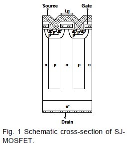
where Id is a drain current, gfs is a transconductance, and Vds is a drain-tosource voltage. The eq. (1) shows that larger Cgd and lower Vth can reduce the turn-off dV/dt when Rg, Id and Vds are fixed. A schematic cross section of a SJMOSFET is shown in Fig. 1. Cgd is determined by the p-base spacing that is related to gate length (Lg). Vth is determined by the impurity concentration of the p-base. In order to increase Cgd and decrease Vth, the expansion of Lg and the reduction of the impurity concentration of the p-base are necessary, respectively.

2.2 Lg dependence
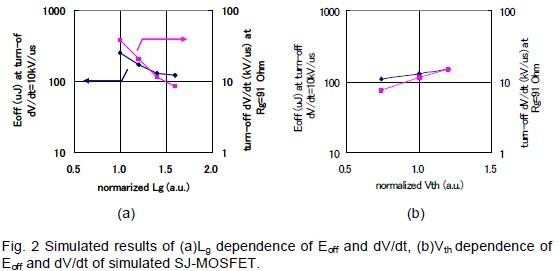
Numerical calculations on the SJ-MOSFET in Fig. 1 were performed. The calculated results of Lg dependence of the Eoff at the turn-off dV/dt of 10kV/us and of the turn-off dV/dt at Rg of 91Ω are indicated in Fig. 2(a). In Fig. 2(a), the value of Lg is normalized by that of our conventional SJ-MOSFET. As shown in Fig. 2(a), the longer Lg can make the turn-off dV/dt lower and this results in the improvement of the Eoff-turn-off dV/dt trade-off. However, the Eoff remains almost the same in the Lg of over 1.4(a.u). This means that optimized Lg is around 1.4(a.u.) for simulated SJ-MOSFET.
2.3 Vth dependense
Figure 2(b) shows the calculated results about Vth dependence of the Eoff at the turnoff dV/dt of 10kV/us and of the turn-off dV/dt at Rg of 91Ω with optimized Lg. The value of Vth is also normalized by that of our conventional SJ-MOSFET. The lower Vth also makes the Eoff-turn-off dV/dt better, but too low Vth makes the SJ-MOSFETsensitive with easily turn-on by noise. Therefore, the optimized Vth is around 0.75(a.u.) as considering the malfunction caused by noise.

3 Experimental Results
3.1 Fabrication process
Based on the above results, an optimized SJ-MOSFET was fabricated by using multiepitaxial growth technique.This technique consists of following sequence. First, a low concentration n-layer is grown on the n-type substrate. Next, n-type and p-type ions were implanted on the nlayer. The growth of n-layer and the ion-implantation were repeated until desired thickness of the drift layer is reached. Then, ion-implanted n-type and p-type region on the each epitaxial layer were connected and n/p-pillars were formed by thermal budget. Finally, SJ-MOSFET is fabricated by conventional double diffused MOSFET (DMOSFET) process on the above SJ structure.This technique enables precise control of the impurity concentration in n/p-pillars because their concentration depends on the precision of the photo lithography and the ion-implantation. Furthermore, this technique can change the distribution of the impurity concentration along the depth direction by layer.
3.2 Device performance
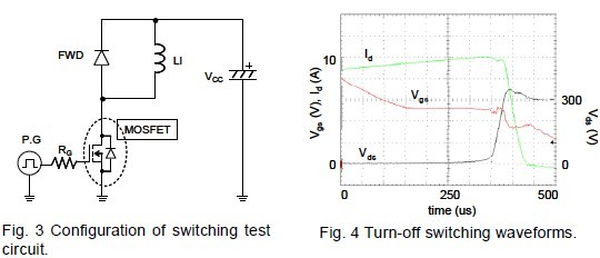
The fabricated SJ-MOSFET had a very low on-resistance of 0.10Ω, which was equal to the RONA of 20mΩcm2, at the breakdown voltage of 680V. Figures 3 and 4 show the configuration of the switching test circuit and the turn-off waveforms of the circuit observed at Rg=91Ω, respectively. A step down chopper circuit is used to estimate switching characteristics of a SJ-MOSFET as the test circuit consisting of Rg, a pulse generator (P.G), a power supply (Vcc), a parallel connected free wheel diode (FWD) and a load inductance (Ll). As shown in Fig. 4,the device exhibited clear turn-off waveforms.
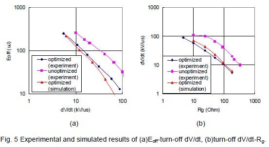
Figures 5(a) and (b) show the experimental results of Eoff-turn-off dV/dt trade-off and turn-off dV/dt-Rg relationship, respectively. The experimental result of the unoptimized SJ-MOSFET and the simulated result of optimized SJ-MOSFET were also shown.

Figure 5(b) exhibites that the dV/dt controllability of Rg in the optimized SJ-MOSFET was improved substantially compared to that of the unoptimized one. In the result, the fabricated SJ-MOSFET obtained an excellent Eoff-turn-off dV/dt trade-off as shown in Fig. 5(a). The value of Eoff was 160uJ at the turn-off dV/dt of 10kV/us and was reduced by about 40% compared to that of the unoptimized one.

3.3 Investigation in electric equipment
In order to evaluate the performance of the fabricated SJ-MOSFET, the device is set to the power factor correction (PFC) circuit in the 400W-class power supply as indicated in Fig. 6, and the power loss is investigated. Figure 7 shows the comparison of power loss in the power supply between the optimized device and the unoptimized one. The input voltage is 115V, the switching frequency is 60kHz, and the output voltage is 390V.
The turn-off loss in the optimized SJ-MOSFET is reduced by about 40% and the total loss is reduced by about 23% compared to the unoptimized one. The power efficiency in the fabricated SJ-MOSFET is 94.5% at 50% of the load factor. (In case of our conventional SJ-MOSFET, the power efficiency is 94.0% at the same load factor.) In addition, the power efficiency is over 94.0% from 20% to 100% of the load factor. This result satisfied “80 Plus specification“ [6] and the fabricated SJ-MOSFET can contribute the energy savings.

References
[1] T. Fujihira : Theory of Semiconductor Superjunction Devices, Jpn. J. Appl. Phys.Vol. 36, pp. 6254-6262, 1997.
[2] G. Deboy et al. : A New Generation of High Voltage MOSFETs Breaks the Limit Line of Silicon, Proc. IEDM, pp. 683-685, 1998.
[3] Y. Onishi et al. : 24mΩcm2 680V Silicon Superjunction MOSFET, Proc. ISPSD’02,pp. 241-244, 2002.
[4] W. Saito et al. : A 15.5 mΩcm2-680V Superjunction MOSFET Reduced On-Resistance by Lateral Pitch Narrowing, Proc. ISPSD’06, pp. 293-296, 2006.
[5] B. J. Baliga : Modern Power Devices, John Wiley & Sons, Inc., pp. 305-314, 1987.
[6] ECOS Consulting : http://www.80plus.org