Inverter stage with a p/n-channel MOSFET combination
Marco Pürschel, Infineon Technologies AG, Germany, marco.puerschel@infineon.com
Abstract
In a modern car a lot of electric drives are visible. From the window lift to electric power steering a broad variety of different power ranges with different motor solutions and different electronic content is present [1]. The inverter to drive these kinds of applications is normal y done with some n-channel MOSFETs, a driver IC, a µ-control er and some communication and supply devices. Typical applications to drive an electric motor are single ended solutions with one power switch, h-bridge topologies or even 3-phase-bridges. As the interface between the µ-control er and the power MOSFETs a driver IC supplies the necessary current and voltage to the MOSFET-gates for safe and predictable switching performance. For automotive applications with its high requirements regarding safety aspects, some protection functions are as wel integrated into the driver IC, short circuit and over temperature protection are just two common examples.
This paper wil focus on a new approach with a p-channel MOSFET as the high side and an n-channel MOSFET as a low side switch. The typical advantages of that setup wil be highlighted, the disadvantages assessed. Special focus wil lie on the driver IC for a p/n-channel combination; a device which is not available on the market up to now.
1.Introduction
Typical drive applications for an electric motor in automotive as wel as in industrial applications contains out of the power stage itself with its typical MOSFETs in a single ended, h-bridge or B6 topology, a driver IC to supply the gates of the MOSFETs, a µ-control er to generate the PWM pattern and some supply and communication devices.
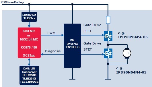 Fig. 1. Schematic of a single ended driving stage
In Fig. 1 a block circuit diagram of a half bridge power stage is visualized. The motor wil be supplied with its current via a high side p-channel MOSFET and a low side n-channel MOSFET for freewheeling. The both MOSFETs wil be driven by driver-IC, which wil amplify the PWM signals of the µ-control er. Typical supply stage for the µ-control er and the communication interface which might be a CAN or LIN transceiver is shown.
With two MOSFETs only, the motor can be just turned in one direction. Some typical applications could be an engine cooling fan, the air-conditioning fan or some pump applications like water pump or gasoline pump.
With the trend towards more electrification in cars, due to the need for reduced fuel consumption, more and more electric motors are used. To make a modern car stil affordable, the cost pressure for automotive ECUs (electronic control units) is high and the tier ones are highly motivated to improve their systems from generation to generation.
In the attached example a p-channel MOSFET is used as a high side switch. Whether this solution wil offer some benefits compared to the classic approach with an n-channel MOSFET as high side and low side switch wil be discussed in the fol owing.
2.Motivation for a p/n-channel solution
Up to 70 (!!!) motor drive applications can be found in a modern car. Depending on the features and the power of the electric drive solution, discrete or integrated components in different topologies wil be used.
For a medium power range (150W to 400W) a discrete solution with a p-channel MOSFET as high side switch and an n-channel MOSFET as low side switch wil offer some benefits on system level.
Main advantage of a PFET versus an NFET (for Infineon MOSFETs it is cal ed SFET) is the fact that the part can be switched on with a negative Gate to Source voltage. Therefore it is a perfect device for al kind of high side switches, where Source of the MOSFET is connected with the supply voltage (for automotive typical y around 12V) of the application. By connecting the Gate of the MOSFET to ground,a negative Gate to Source voltage is given and the device can be easily switched on.
But there is one main disadvantage of a p-channel MOSFET compared to an n-channel MOSFET. This is the mobility of the holes in comparison to the electrons which would result in higher on-state resis tances. Therefore for the same resistance the area of a p-channel MOSFET is bigger compared to an n-channel device, resulting in higher component costs.
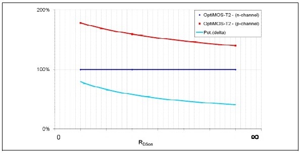
Fig. 2. Comparison of cost of PFET vs. SFET as a function of the on-state resistance
In Fig. 2 the difference in percent between an n-channel (SFET) and a p-channel (PFET) MOSFET as a function of the on-state resistance is shown. The lower the on-state resistance of the MOSFET wil be, the higher is the difference in cost between both devices. This additional amount of money has to be compensated somewhere on system level. The device which can be simplified is the driver IC by saving the charge pump and its corresponding devices.
2.1. The p-channel MOSFET
A MOSFET is a unipolar device where only one kind of charge carriers is responsible for the current
flow; either electrons for an n-channel device or holes for a p-channel device.
Electrons mobility = 1400cm²/(Vs)
Holes mobility = 450cm²/(Vs)
[2]
The difference in charge carrier mobility determines in the first step the different on-state resistances of the MOSFETs. Means: A p-channel MOSFET has 1400/450 = 3.1 times higher values. For a state of the art MOSFET this factor is smal er, simply due to the fact that the resistance of the product is not only determined by the resistance of the silicon but as wel by the package (bond wires, pins, …) which is the same for n and p-channel MOSFETs. In Fig. 3 the difference in on-state resistance between the latest n-channel and p-channel technologies in 40V from Infineon is shown. Depending on the die size of the device, the advantage in RDSon of the SFET is in between 2.5 and 1.75.
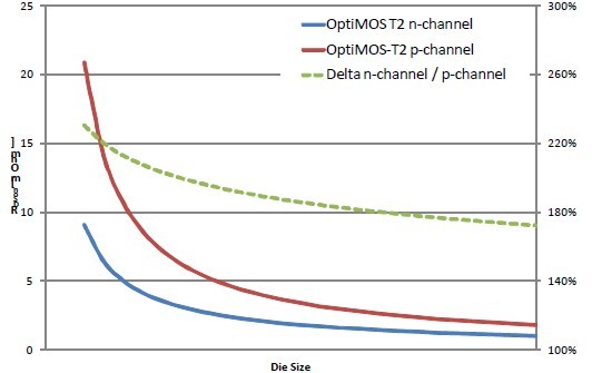
Fig. 3. RDSon comparison OptiMOS-T2 n-channel vs. OptiMOS-T2 p-channel
Nevertheless with this latest p-channel technology it is possible to offer very low ohmic MOSFETs in standard industry packages like the DPAK or the D²PAK. Values down to <3mOhm for a 40V device are possible which is in the typical range for a lot of automotive electric drive applications.
2.2. The driver IC
To drive the Gates of the MOSFET a dedicated driver IC for p-channel and an n-channel MOSFET is mandatory. It acts as the interface between the µ-control er and the power MOSFETs. The Driver IC,level shifts, amplifies, and buffers the control signals coming from the µ-control er to provide the gate charge for the high side and low side MOSFET.
With the new IPN10EL-S the first automotive qualified driver IC for a p/n-channel combination wil be available on the market.
The IPN10EL-S is a gate driver IC dedicated to drive one p-channel and one n-channel MOSFET.
Typical y these two MOSFETs are used as one leg in a bridge topology forming the converter for DC motor drives in automotive applications. The driver IC contains an interface to the µ-control er, adjustable dead time generation and basic protection features like short circuit, under voltage and over temperature.
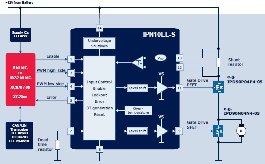 Fig. 4. Block diagram PN-driver IC
Fig. 4 shows a typical application example with some 5mOhm MOSFETs. Applications for that could be a low end engine cooling fan in the 300W range.
The principle functionality of the driver IC is explained in the fol owing.
By applying a high signal on the enable pin (1), the IPN10EL-S wil be activated and the two output stages can be used. By leaving the dead time pin (7) open, the high side MOSFET and the low side MOSFET can be individual y control ed by the PWM high side (3) and PWM low side (4) pin. Any kind of PWM pattern can be generated.
The IPN10EL-S offers a flexible concept for the dead time generation. Both driver stages can be 100% control ed individual y, thus providing ful comparability to any application requirement (e.g. driving an injector where the load is connected between the high side MOSFET and the low side MOSFET).
Nevertheless it is a must in bridge applications to avoid cross current, that the external high side and low side MOSFET are not turned on at the same time, leading to a directly short circuit of the battery voltage to ground. Therefore a dead time has to be defined between the switching transitions of the two MOSFETs.
The IPN10EL-S offers the possibility of an internal dead time generation / shoot trough protection. By applying an external resistor between the dead time pin (7) and ground, the value for the dead time wil be determined. Using the internal dead time generation, the PWM high side input wil be disabled. The MOSFTEs wil be switched on and off alternating by the PWM low side input only.
The implemented protection features contains of over temperature protection of the IC, under voltage protection to operate the MOSFETs within specification (different levels can be set for logic and normal level MOSFETs) and a basic short circuit protection.
The device is dedicated for low end applications with limited protection features. Therefore just a basic short circuit protection is implemented. The voltage drop via a high side shunt resistor is measured. By reaching its internal reference voltage, the driver IC wil switch off both MOSFET gates.
3.System approach
The question where a p/n-channel approach wil offer some benefits compared to a standard n/n-channel solution can be answered by a cost comparison on system level. Defining the system, it might be the easiest way to focus on the main components of a driver stage which wil be influenced by the selection of a p-channel MOSFET; the driver IC and the power MOSFETs. On that level the solution should be price competitive!
The p-FET is more expensive compared to its n-FET equivalent, which means the driver IC has to be cheaper. With a PFET no charge pump or any similar complex circuitry is necessary. It enables a very simple drive circuit and wil save money; either on complex driver- or system ICs or on discrete components.
So the main target of the driver IC would be to offer on a system level a competitive solution compared to today’s standard solution with n-channel MOSFETs. The cost adder of the PFET has to be compensated.
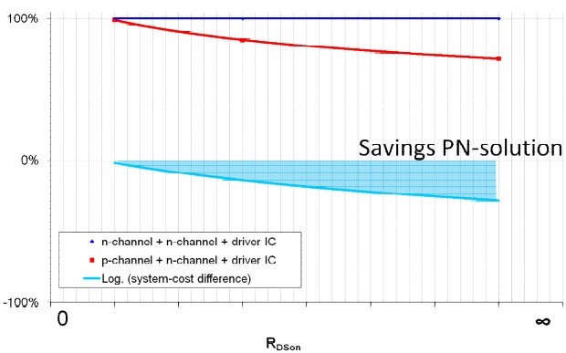
Fig. 5. Comparison of system-cost of a p/n-solution with an n/n-solution
By comparing two n-channel MOSFET with a drive IC with one p-channel plus one n-channel plus one driver IC, the break even is in the 3mOhm range (see Fig. 5). The diagram is showing as the reference line (100%) the n/n solution in blue and in red the p/n solution. On the y-axis the cost in percent is shown, on the x-axis the RDSon of one MOSFET shown. The area, where the red line is below the blue one, offers lower cost for the p/n solution.
The advantage of a p/n solution wil increase to higher on-state resistances due to the fact, that the charge pump can be assessed as fix amount of money, nearly independent on the used MOSFETs (different gate charges would require of course different gate currents and different charge pumps, but in reality al driver IC are designed in a very similar way).
In addition to that pure cost comparison counts some “soft facts” for the p/n-solution. A charge pump is always a source of EMI problems, due to its high switching frequencies. Due to the absence of the charge pump, the EMI behaviour should be improved.
Some external components (resistors or capacitors) can be saved, resulting in additional cost down and some smal savings of board space.
Final y the PFET as a high side switch wil offer the ful range of duty cycle without any constrains. Everything in-between 0% and 100% is possible; the p-channel MOSFET can be turned on as a high side switch by connecting the Gate with Ground.
Target applications for such a p/n solution would be motor drives in the car in the low to medium power range (typical y 150W to 400W). Some examples would be HVAC blower fan, low power engine cooling fan, wiper or window lift.
Dependent on the used motor and the requirements of the application, one, two or three p/n-legs have to be used.
4.Conclusion
The p/n-channel MOSFET and driver approach for automotive electric drive applications offers a new cost competitive solution on the market.
Due to the fact that p-channel MOSFETs are always larger compared to its RDSon equivalent n-channel part, the PFET is more expensive. That cost adder has to be compensated by savings on the driver IC side to offer an attractive solution. An internal assessment leads to the conclusion that this concept wil pay off for devices with an RDSon larger then 3mOhm MOSFETs. Typical power range is accordingly 150W to 400W for an electric drive application.
Despite of the cost benefit some soft features on application level could be highlighted in addition. The absence of the charge pump with its high switching frequencies wil improve the EMI behavior of the system. Some external components can be saved which wil lead to reduced board space and simplified layout.
Infineon offers the first time a real high power p-channel MOSFETs in the 40V league in combination with the first p/n-channel driver IC. Bottom line, the p/n driving stage for electric drive applications offers a new approach on the market which might be considered in the future for the designer of automotive ECUs.
5.References
[1] Andreas Kiep et al © 2005 SAE International: “Seamless Solution for EPS: Electronic Power Steering”
[2] http://en.wikipedia.org/wiki/Electron_mobility