
Innovative half bridge control technology for high power density DCDC converter application
Owen Jiang, Texas Instruments Semiconductor Technologies (Shanghai) Co., Ltd., Shenzhen,
P.R.China, owen-jiang@ti.com
Abstract
Recently, more & more green environment requirements drive the power supply performance towards high power density /high efficiency /low cost / lowest standby power consumption etc. therefore the power designer put forwards much more requests for controller IC . Some of novel control technologies are come out and researched by peoples little by little. This paper describes one innovative half bridge control technology –Integral cycle control technology. This is different with other half bridge control solution.
The basic principle and concept is presented. And it can be used to realize higher efficiency and lowest standby power consumptions as well. This paper also give one completely comparison between LLC resonant half bridge and integral cycle control method. Finally one experiments results comparison based on 90W high density adapter scheme is presented.
1. Background Introduction
1.1. The systems requirement
90W high efficiency adapter has been used widely from notebook to medical , and even other electrical end equipments . and from Energy saving view, much more high efficiency requests for both whole load range and standby power consumption becomes important greatly.
Based on Energy star 2.0 SPEC, under no load condition, the input power should be less than 0.5W on wide input range from 90V to 265V. as for normal operation mode, the average efficiency is requested , which means to test 25%/50%/75% and 100% load four condition , and to get one average value . this average efficiency should be large than 85%. So one good high efficiency adaptor solution should be to meet standby efficiency target as well as the average efficiency target .
Currently , most of high efficiency adapter used Boost PFC + LLC resonant half bridge topology as main solution and matched with different external or internal standby circuit to meet high efficiency request. But Secondary rectifier MOSFET driver is a headache for LLC application. And this paper will introduce one creative idea , and it is based on buck PFC + ICC half bridge topology as followed Figure 1 show
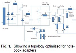
This architecture uses a buck PFC stage, ([1], [2],[3], [4]) with the “mid-cycle” voltage on the bulk capacitor typically chosen as 80V.
The isolation DCDC stage as shown is a halfbridge primary, with self-driven synchronous rectifiers.
2. ICC control concept
2.1. Voltage second unbalance issue in half bridge & pulse set
In symmetrical half bridge application, current mode control will leads to un-balance issue . so voltage mode control is adopted by more & more IC designers. But there still has potential voltage second unbalance issue specially when load transition between no load and full load , or under over current condition happened.Normally one current sense transformer is need to realize peak current cycle by cycle limitation as protection method. But this approach cost additional current sense transformer . if there is one approach can make sure that upper & lower MOSFET duty cycle keep symmetrical , that will remove unbalance issue .
A “balanced” pulse-set is to meet this requirement.
A simple case of such a pulse set is where the lower FET is driven initially for ¼ period,then the upper FET for ½ period and the lower FET then for ¼ period. This ensures nearzero net magnetizing current.
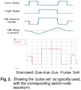
From whole cycle view , this pulse set looks like 50% symmetrical duplicated upper & lower MOSFET driver signal to guarantee that voltage across capacitor always balance under all kinds of condition. So the switching behavior is near to DC transformer .
2.2. Hysteresis control
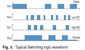
In fact , Integral cycle control(ICC) is one of voltage hysteresis control mode and to use balanced pulse set as basic dutcycycle unit. The output voltage is sensed and compared to a reference value by a comparator on the secondary side, and the comparator output drives a digital opto-coupler. When the output voltage is below the regulation level, the comparator output is high and the opto-coupler is not driven; when the output voltage exceeds the regulation level, the comparator output goes low and turns on the opto. In this way, the output comparator acts like a simple 1-bit A/D converter. The opto-coupler feeds the digital feedback information to the primary side across the isolation barrier. The optocoupler output signal to FB is high when Vout is below regulation level, and low when Vout is below the regulation level. Figure 3 show basic switch logic for both primary side MOSFET and secondary side control.
In normal mode, the controller monitors the FB pin to determine the switching cycle mark/space ratio. When FB is found to be high, a switching cycle is commenced. Every time a switching cycle is commenced, it is completed fully, regardless of the FB pin level. During each current switching cycle, FB is monitored to determine whether or not a subsequent switching cycle should be delivered. If FB stays high, then another switching cycle is delivered contiguously. If FB goes low, then switching ceases or drops out at the end of the current cycle. While delivering switching cycles, FB is polled once every switching cycle, or approximately every 8 us. Once switching ceases at the end of the cycle, FB is monitored while the controller waits for the next FB high transition to indicate that switching should recommence.
2.3. Synchronous rectifier control
When operating with synchronous rectifiers in this fashion, it is important that the waveform be clamped in the “off” time. If this is not the case, a “Royer Oscillator” condition may occur where the synchronous rectifiers can drive an oscillatory condition. The simplest way of effecting clamping is usually by loading a winding or windings which can also be used for bias supply.
At power levels common in notebook adapters (e.g. 90W) the clamp functionality can be implemented simply using a small (SOT23) MOSFET driven directly from the controller.
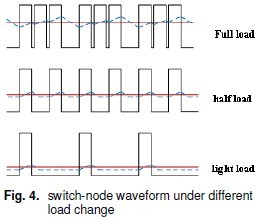
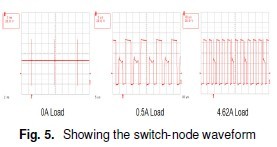
The control approach at higher loads results naturally in a concatenation of pulse-sets, which results in extended periods of square-wave type operation, with each period of such operation commenced and terminated with a stub-pulse. A dropout occurs to effect regulation, and this is as shown in figure 4.
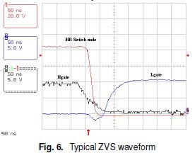
The ICC algorithm, with appropriate design of drive timings, achieves zero-voltage switching on a majority of the transitions. The approach is however particularly well suited to usage with a buck PFC stage where operation is from 80V, and loss of ZVS operation on some transitions does not result in excessive dissipation.
3. Advantages compared with LLC resonant converter
Compared with LLC , ICC has following advantages:
1) Very high efficiency result for whole load range. First is number of switching cycles delivered is approximately proportional to load in DCM, more like conventional PWM in CCM. It help to minimise switching loss, gate drive & transformer core losses at light to moderate loads.
2) Second is each switching cycle designed to be maximally efficient. That is effectively DC transformer when switching always. the switching dutycycle close to 50%, small dead time to achieve soft-switching ZVS for most load condition easily .
3) Third is switching frequency decreased with load decreased linearly. ICC is similar with LLC , both are PFM –pulse frequency modulation in principle . but the different is LLC will increase switching frequency when load decreased.
And ICC is reverse . with Load decreased, the ICC controller drop more pulse set , looks like decrease switching frequency linearly . also it is not like burst mode , it will work under whole load range. So it can deliver high efficiency performance for whole load range .
4) High duty-cycle square transformer waveforms – very easy self-driven forward SR MOSFET on secondary side. Because ICC approach use pulse set as basic driving signal unit. This make sure one 50% high dutycycle square transformer waveform. So it can be easily to use as self-driven secondary side synchronous rectifier MOSFET solution.Also one Clamp function is adopted to shutdown SR driver so as to avoid fault turning on SR MOSFET.
5) Fast transient response for dynamic load change request. Because ICC use hysteresis control and no complex compensation circuit. So it can gain very good transient performance compared with LLC.
4. Experiments Data
4.1. Technology Implementation
The ICC approach – optimally used in conjunction with a buck PFC stage – can be used to design very high-efficiency notebook adapters. An example 90W reference design for universal input and nominal 19.2V output is as shown in figure7.
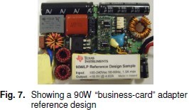
This reference design can exhibit power density of approximately 1.1MW/m3.
To achieve such power density naturally requires significant component engineering, including appropriate choice of magnetics components. The converter however has to be very efficient ->92% - if the case temperature is to be kept below limits as imposed.
4.2. Performance Data
The aggregate efficiency is as shown in figure 8.
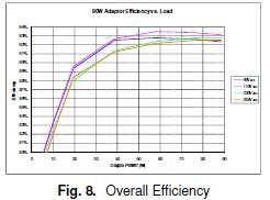
This shows the aggregate performance, with the efficiency seen to be largely invariant with line under high-load conditions. The issues of efficiency roll-off at low line, as are a major issue with boost-type converters, are thus much less relevant with this approach.
Within this implementation, the buck PFC stage can be designed for 96%+ efficiency over line at full-load conditions. The ICC-stage needs to have comparable efficiency to achieve the overall efficiency requirements, and the high efficiency that is obtainable over load is as shown in figure 9 & 10.
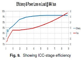
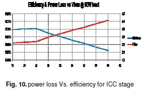
Figure 9 & 10 shows the ICC half bridge stage efficiency and power loss performance based on whole 90W adapter design (Buck PFC +ICC half bridge ). From half to full load , the ICC can deliver above 96% high efficiency result . even under light load , it can gain above 75% efficiency as well.
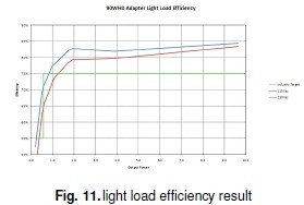
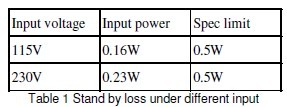
Figure 11 and table 1 shows the stand by performance based on whole 90W adapter design (Buck PFC +ICC half bridge ). Under no load condition , buck PFC and ICC both work at burst mode mode which make sure lowest stand by loss performance.
The design approach as shown is well suited to the design of notebook adapters. The usage of direct-driven synchronous rectifier approaches minimizes cost and component count, and allows a robust design implementation. The transformer can easily be designed for low common-mode noise generation, aligned with the usual requirements in adapters for smaller common-mode filtering components, allowing minimal AC-line leakage. Having a simple control approach –valid from no-load through to full-load without complex mode-switching – is also conducive to easy implementation.
5. Summary
The usage of ICC type approaches – particularly in association with a buck PFC stage – can give an elegant, low-cost design for notebook adapters. Adapter designs at very high-efficiency and high-density can be realized, or alternatively it is
possible to implement designs at very low cost. Specially compared with LLC control from principle and experiments result , ICC has better efficiency and standby power performance
6. Literature
[1] – R Redl, A Kislovski, B Erisman, Input Current Clamping – an Inexpensive Control Technique to achieve compliance with Harmonic Regulations, 078033304, IEEE Applied Power Electronics Conference, 1996, pp 145-151
[2] – G. Spiazzi, Analysis of buck converters used as Power Factor Preregulators. IEEE Power Electronics Specialists’ Conference, 1997
[3] - G. Young, G. Tomlins, and A. Keogh, "An acdc converter," World Intellectual Property Organization,International Publication Number WO 2006/046220 A1, May 4, 2006.
[4] - Huber, L., Gang, L., and Jovanovic, Milan M.– Design-Oriented Analysis and Performance Evaluation of Buck PFC Front-End – IEEE Applied Power Electronics Conference, 2009
[5] – UCC29900 datasheet, Texas Instruments